

There is a wide variety of facilities and equipment registered by universities, etc., nationwide participating in ARIM. We have equipment that accelerates research and development, such as electron microscopes that can observe atomic-level dimensions, nuclear magnetic resonance equipment that can analyze the structure of compounds, and mass spectrometers that measures the mass of ions.
(BL22XU) Surface chemistry experimental apparatus (BL23SU) Soft X-ray photoelectron spectrometer (BL23SU) Scanning Transmission X-ray microscopy apparatus (BL23SU)
DEVICE
Energy-dispersive XAFS measuring station
[BL14B1]
In addition to conventional X-ray absorption spectroscopy (XAFS) measurements using a double-crystal monochromator, dispersive XAFS measurements using a curved analyzing crystal can be performed. In conventional XAFS measurements, a 36-element semiconductor detector is used in the fluorescence method. Sample temperature range from 20 K to 1073 K can be covered.
Control of atmosphere containing carbon monoxide and nitrogen oxides is possible by using a gas control system. Gas composition analysis using a quadrupole mass spectrometer is also available.
Typical application
In-situ and real-time observations of catalytic reactions.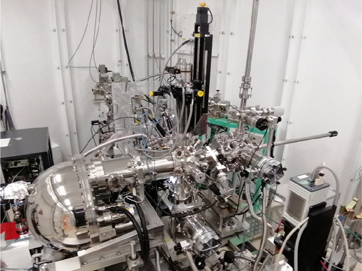
Hard X-ray photoelectron spectrometer
[BL22XU]
Hard X-ray photoelectron spectroscopy can reduce the effects of surface contamination and obtain bulk information. In particular, it is effective for electronic structure analysis of samples whose surfaces are difficult to clean and devices with nanoscale multi-layered structures. In addition, it is possible to select the excitation energy (from 6 keV, 8 keV, and 10keV) and detection depth according to the purpose. Damage analysis of radiation-resistant spin-driven thermoelectric elements is an example measurement.
Typical application
The Damage Analysis for Irradiation Tolerant Spin-Driven Thermoelectric Device
XAFS measuring station
[BL22XU]
XAFS measurements using high-brilliance, high-energy X-rays from an undulator are possible. Time-resolved quick x-ray absorption fine structure (Quick-XAFS) measurements are also possible. Various detectors such as ion chambers, NaI scintillation detectors, and Ge semiconductor detectors are available. A cryostat for low temperature measurements is also available.
Typical application
Analyses of structures and electronic states for functional molecular design.
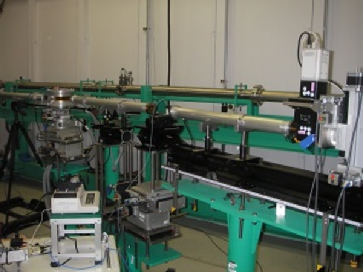
The apparatus for imaging and measuring material stress
[BL22XU]
Imaging measurements of strain and stress distribution mainly in metallic materials are possible.
Using the high-temperature (as high as 900 ℃) and load (maximum of 5kN) apparatus, in-situ measurements are also possible.
Simultaneous use of multiple two-dimensional detectors enables time-resolved measurements at a maximum speed of 200 Hz for strain/stress measurements, and 2000 Hz for imaging measurements.
Typical application
Evaluation of stress, strain, dislocation density in metal materials under deformation, melt solidification phenomenon observation during laser processing.
κ-type X-ray diffractometer
[BL22XU]
In addition to the conventional 6 axes, the κ-type diffractometer has a rotational axis in the horizontal plane for the entire system, making it suitable for surface structure analysis. Simultaneous measurement of electrochemical properties using a potentiostat, etc., is possible. The sample temperature can be lowered to 10 K using a He circulation type refrigerator and raised to 1000 K when using an electric furnace.
Typical application
ln-situ observation of the surface structural change of a secondary battery electrode during charging/discharging.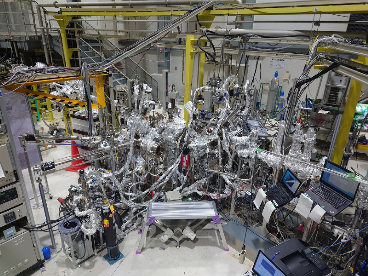
Surface chemistry experimental apparatus
[BL23SU]
In-situ observation and real-time measurements of the dynamics of chemical reactions such as adsorption-desorption, oxidation-reduction, etc., on metal and semiconductor surfaces are possible. In the surface preparation chamber, the surface can be cleaned by Ar ion sputtering and heating up to 1450K. LEED and AES are also available for reconstructed surface and chemical composition observation.
The gas dozer and supersonic molecular beam apparatus can supply gas molecules with various kinetic energies to sample surfaces.
In addition to synchrotron radiation photoelectron spectroscopy, reaction dynamics can be observed with thermal desorption analysis, STM/AFM, and LEED/AES.
Typical application
formation processes of graphene, insulator layers on SiC surfaces.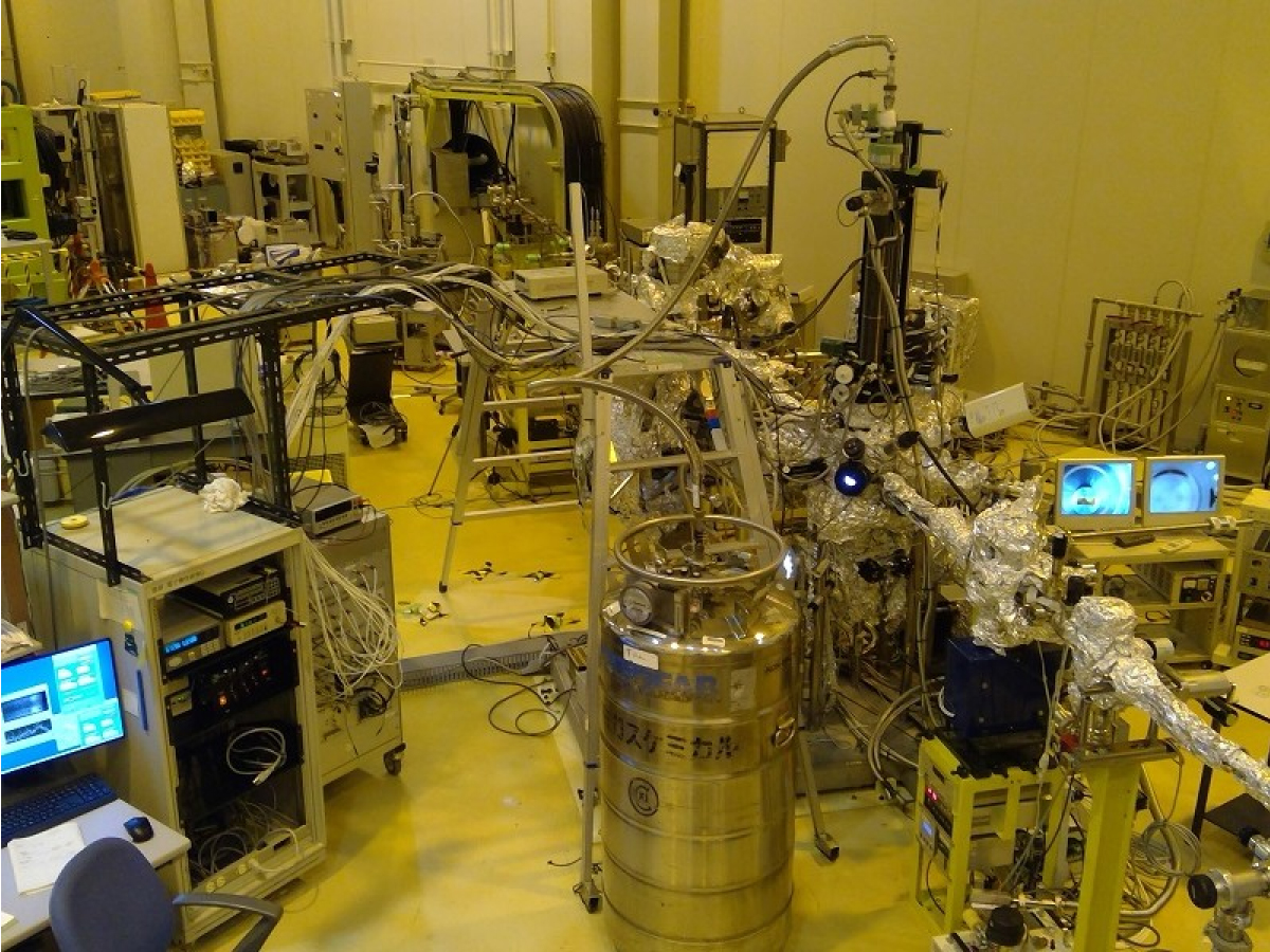
Soft X-ray photoelectron spectrometer
[BL23SU]
High-resolution photoelectron spectroscopy can be used to measure the electronic structures, chemical bonds, etc., of strongly correlated electronic materials such as rare-earth elements, transition metals, and uranium actinides.
Angle-resolved photoemission spectroscopy (ARPES) measurements are also available, allowing detailed studies of the electronic structure of rare earth and 3d transition metal compounds.
SR energy: 400-1500 eV
Energy resolution: 50-200 meV
Sample temperature: 6-300 K
Typical application
Electronic structure studies of high-efficiency thermoelectric conversion materials.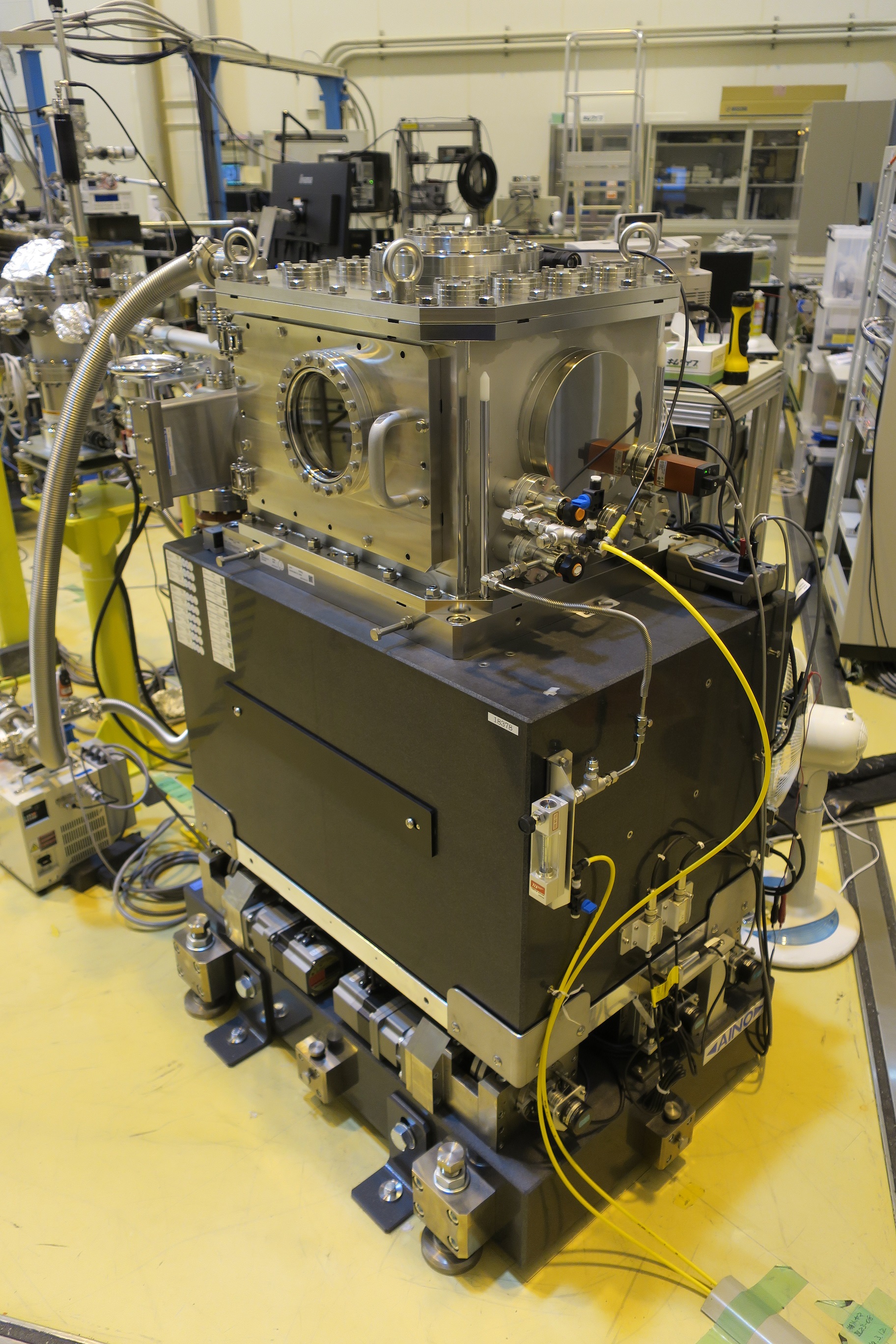
Scanning Transmission X-ray microscopy apparatus
[BL23SU]
STXM is an element-selective chemical analysis tool with nanoscale spatial resolution. A two-dimensional mapping of transmitted x-ray (i.e. absorption) intensity can be obtained by irradiating a sample with soft x-rays focused to several tens of nm by a Fresnel zone plate and scanning the sample. By measuring the photon energy dependence of the two-dimensional mapping, absorption spectra at each position can also be obtained. Therefore, STXM is a powerful technique for the analysis of microparticles and samples with inhomogeneity and one can analyze the spatial distribution, valence states, and chemical bonding states for a wide range of elements, including lanthanides, actinides, 3d transition metals, as well as nitrogen and oxygen in organic compounds.
Available photon energies: 400-1900 eV
Best spatial resolution: 30 nm (in case of 25nm FZP)
Sample temperature: 300 K